
5. Signals in Electron Microscopy#
5.1. Electron scattering#
In the electron microscope, energetic electrons travel down the electron column in vacuum until they encounter the sample. There they may cross the vacuum-sample interface and penetrate into the sample. In the sample, the electrons will interact with the sample material, which can lead to emission (including transmission) of electrons, X-rays, and visible photons. All these can be used as signal that we detect to visualize or characterize the sample. To understand these signals and what kind of information they bring, we need to develop a basic understanding of electron-matter interaction. For our purposes here, it is sufficient to look at the interaction of electrons with individual atoms in the material and consider the orbital model for the composition of the atoms.
5.1.1. Orbital model and electron-atom interactions#
5.1.2. Elastic and inelastic scattering#
Based on the electron-atom interactions explained in the preceding section, we can see that the incoming primary electron (i.e. an electron from the electron beam) can leave the sample in a variety of ways. Important for EM is the distinction between primary electrons that have undergone no or only elastic scattering interactions and primary electrons that have undergone inelastic scattering interactions. A transmitted electron is an electron that has passed through the sample without any change in direction. An elastically scattered electron will have changed direction and momentum but will not have lost any energy. The electron feels the combined charge of electron cloud and nuclear charge and is attracted by the nuclear charge. However, due to its velocity and kinetic energy, it does not collide with the nucleus but is only deflected. A backscattered electron is an elastically scattered electron where the scattering angle is larger than 90 degrees. These thus leave the sample on the same side facing the incoming electron beam. We will in the remainder refer to this as the upper side of the sample. Consequently, the bottom side of the sample is the side where transmission electrons exit.
An inelastically scattered electron is an electron that did loose energy on its way through the sample. This is mostly due to collisions and energy transfer with other electrons in the orbits in the sample material. The energy lost in the inelastic scattering process is transferred to electrons in the material and thus leads to low energy electrons in the material (which if they escape are the secondary electrons) or the emission of X-rays or visible photons. The amount of energy lost in a single inelastic scattering event is in most cases relatively small. Thus a primary electron may undergo multiple scattering events on its way through the sample.
Inelastically scattered electrons will exit the sample at the bottom side, however an inelastically scattered electron may undergo a strong elastic scattering event later, leading to a >90 degrees deflection. Thus, also some of the backscattered electrons may have undergone inelastic scattering events. In addition, of course a backscattered electron may also undergo inelastic scattering after the elastic scattering event. As a result, a fraction of the backscattered electrons will have an energy slightly lower than the primary beam energy, which we have also seen in the electron emission spectrum in Section 5.1.1.
5.1.3. Interactions preserving coherence#
For applications where we want to exploit the electron wave character for imaging, e.g. phase contrast imaging in TEM and electron diffraction, we can only use electrons that have preserved coherence after interacting with the sample. Cleary, inelastically scattered electrons, where the primary electron has lost energy have become incoherent. Transmitted electrons are still fully coherent. Elastic scattered electrons may also be coherent unless they have undergone additional weak inelastic scattering. Fig. 5.1 gives a complete sketch of all different kind of electrons exiting the sample. We have to note here that in order to use coherence in a measurement, sufficient spatial and temporal coherence has to be assured in the beam, otherwise the contributions from different electrons will still not be sufficiently in phase with each other.
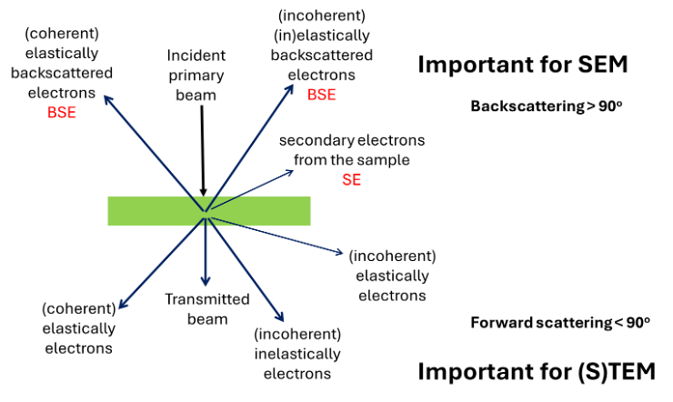
Fig. 5.1 Overview of all possible electrons exiting the sample as a result of scattering with their nomenclature.#
Finally, we should note that as an electron penetrates deeper and deeper into the sample, it will undergo more and more scattering events. Ultimately, the electron will have lost all its energy and not be able to escape the sample anymore. Thus, the picture sketched in Fig. 5.1 only holds for relatively thin samples. We will see later that how thin this can be is related to the primary beam energy and whether or not one is interested in coherence. For thick, or bulk, samples, only SEM is possible.
5.1.4. The scattering cross section#
The scattering of electrons in the material is a probabilistic process: an electron will not interact with all atoms it encounters. The scattering probability is thus an important quantity for evaluating electron scattering. Also, this scattering probability is related to the average distance an electron can travel before it undergoes a scattering event. This distance is what we refer to as the mean free path of the electron.
The scattering probability is expressed in the scattering cross section. This cross section does not represent an actual physical cross section, but rather is the effective cross section an atom or material would have if the probability for interacting would be one. So if a hypothetical atom would have a physical cross section of \(10 pm^2\) and the probability for scattering would be \(0.1\), the scattering cross section would \(1 \: pm^2\). Thus, the scattering cross section is given by:
where r is an effective radius of the atom, typically much smaller than the distance between neighbouring atoms.
For elastic scattering, the effective radius is given by:
where \(Z\) represents the atomic number, i.e. the amount of positive charge (protons) in the nucleus, \(\Delta V\) the potential difference at which the electron has been accelerated and \(\Theta\) the angle at which the electron has been scattered. We thus see that larger nuclear charge increases the probability for elastic scattering reflecting the fact that elastic scattering results from Coulomb interactions between the electron and the nucleus. Further, we see that the elastic scattering becomes less likely for increasing electron energy and for larger detection angles.
For heavier atoms, with a higher atom number, elastic scattering will be stronger. For a higher acceleration voltage, the electrons will scatter less, giving a smaller interaction cross-section. This is also true for inelastic scattering and higher primary electron energy can thus be linked to less radiation damage in the sample. However, the precise dependence of elastic and inelastic scattering cross sections on primary electron energy may differ and optimized conditions will thus depend on the type of signal that is detected and from which elastic or inelastic scattering process (and respective cross section) this signal originates from. In other words, an optimum is obtained for that electron energy at which the most signal is detected with the least damage. Ultimately, this is determined by the ratio between the cross sections for the process that lead to signal generation and the cross sections that lead to damage. If we consider multiple scattering processes, an overall scattering cross section can be obtained by summing the cross sections of all possible scattering processes. Thus, the total electron scattering cross section, \(\sigma _t \), is given by the sum of elastic and inelastic cross sections: \(\sigma _t = \sigma _{elastic} + \sigma _{elastic}\)
5.1.5. Scattering angles elastic vs inelastic#
From equation (5.2), we can also see that scattering into high angles is unlikely and the more so for lighter (i.e. lower atomic number) atoms. The angular dependence of the scattering cross section is important as our detector will only accept a certain range of scattering angles, depending on the detector geometry and position. We should realize that the scattering angle Θ is here defined as the angle with respect to the incoming electron trajectory, see Fig. 5.2. Inside our sample material, this angle may thus differ depending on the angle under which the electron entered the material and also whether or not the electron already underwent previous scattering events. However, in our measurements, we detect electrons with a macroscopic detector at a certain position with respect to the electron microscope axis. In this case, \(\Theta\) is the angle with respect to the axis. Also, we do not detect electrons at a specific (two-dimensional) angle, but rather detect all electrons that are emitted in a (three-dimensional) solid angle that comprises all scattering angles that make it to the detector (see Fig. 5.3). This solid angle is given by:
An incremental change in scattering angle \(d \Theta\) will, according to equation (5.2), lead to an incremental change in scattering cross section \(d \sigma\). Using the relation between scattering solid angle and scattering angle, we can see that the differential of the scattering cross section over solid angle is given by:
The angular dependence of the cross section can be plotted for a particular atom and for the different types of electron scattering. As can be seen in Fig. 5.4, the cross section can substantially differ as a function of emission angle between elastically and inelastically scattered electrons. For elastic scattering, the cross section is relatively high at small angles and decreases rapidly for larger scattering angles. For inelastic scattering, however, it stays relatively constant for a large angular range and then decreases rapidly. A further optimization of the experiment besides selecting electron acceleration voltage may thus be the choice of scattering solid angle captured by the detector. An appropriate selection of solid angle of detection may maximize signal electrons and effectively filter out electrons generated by other scattering processes. Insertion of an aperture (ring) may also help filtering electrons emitted in a specific solid angle.
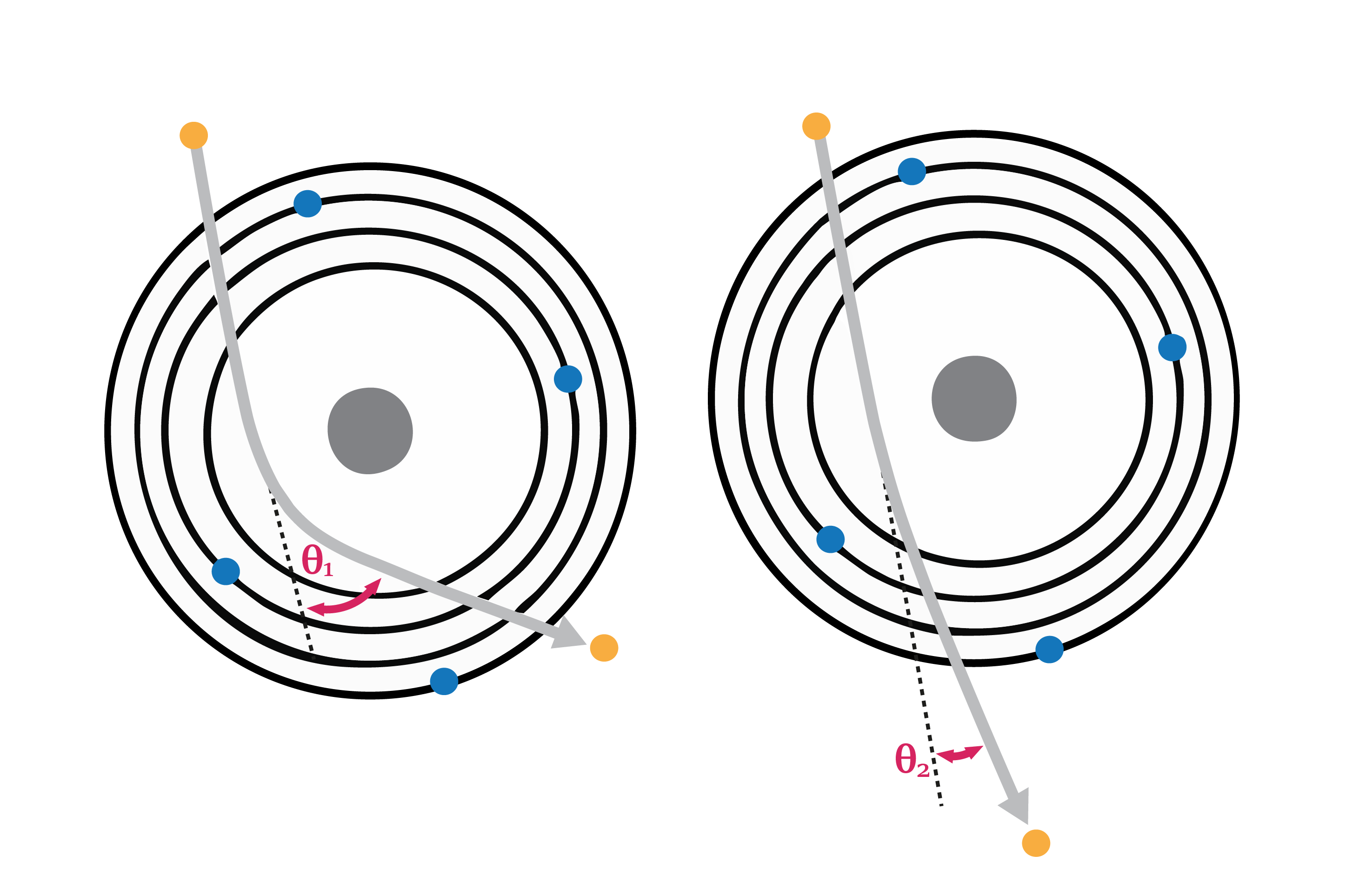
Fig. 5.2 The scattering angle Θ is defined with respect to the direction of the incoming electron.#
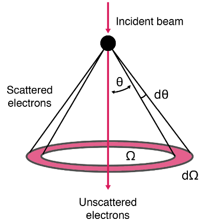
Fig. 5.3 The scattering solid angle Ω represents the three-dimensional cone spanned by all (two-dimensional) scattering angles Θ.#
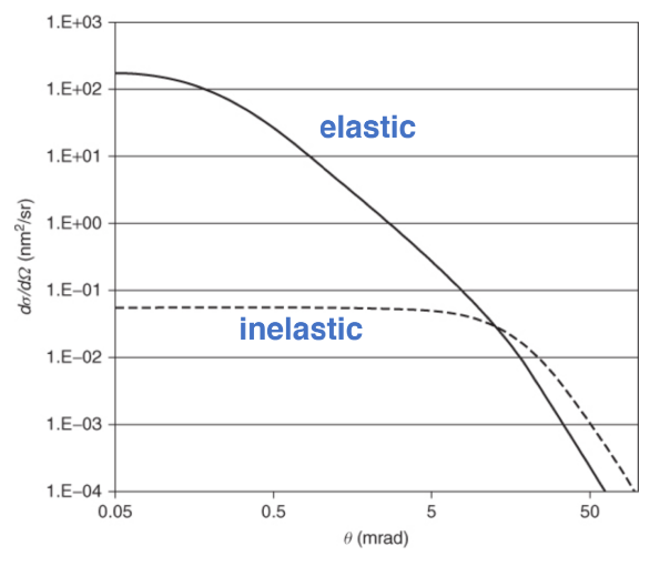
Fig. 5.4 The angular dependence of differential scattering cross section for carbon at a primary electron energy of 100 keV. The behavior of elastic versus inelastic cross sections can be seen to differ considerably.#
5.1.6. The mean free path#
To represent scattering inside a material, we need to extend the scattering cross section formula for a single atom to the collection of atoms present per unit of volume. The total scattering cross section is then simply given by \(\sigma _t = N \sigma _{atom}\) where \(N\) is the number of atoms per unit volume and thus:
where \(N_A\) is Avogadro’s number, \(\rho\) the material density and \(M\) the molar mass (or molecular weight) of the material. From this equation, we can see that the total scattering cross section is expressed in unit of inverse length, i.e. \(1/m\). To determine the total scattering of a specimen \(\Sigma _t\), we can thus multiply its total scattering cross section by the specimen thickness \(d\):
We have previously established that the scattering process is probabilistic and that the scattering cross section represents the probability for an electron to scatter. The total scattering cross section is directly and inversely related to the mean free path \(\Lambda\), the average distance an electron travels before scattering or in other words the average distance between scattering events:
Because of the probabilistic nature of the scattering processes, electron trajectories inside materials cannot be deterministically calculated. Instead, we have to resort to so-called Monte Carlo simulations. In a Monte Carlo simulation, a free travel distance is picked from the probability distributions of all scattering events (i.e. the scattering cross sections). The electron is then, in the simulation, allowed to travel over that distance after which direction and energy (and thus velocity) are altered based on the scattering process. The process is then repeated and this continues until the electron crosses the material-vacuum interface (thus leaves the material) or has lost all its energy in which case it is absorbed in the material. If this process is repeated for many electrons, the resulting scattering pattern will resemble the actual electron scattering in an experiment with many electrons. Also, it gives an indication for the volume inside the material in which electrons may travel and interact and where interactions are most likely to take place. Fig. 5.5 gives an example of the results of such Monte Carlo simulations.
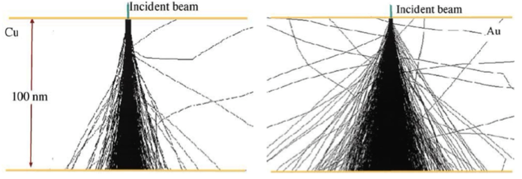
Fig. 5.5 Electron trajectories from Monte Carlo simulations in two different materials, copper (left) and gold (right). Each line represents the path of a single electron. Upon comparison between the two materials, the atom number and scattering angle dependencies in equation (5.2) are clearly recognizable in the results: the results for the gold slab show more scattering (shorter trajectories between scattering events) and scattering at higher angles, where the trajectories in copper remain closer to the incident electron axis consistent with the higher atom number of gold (\(Z_{Au} = 79\) vs \(Z_{Cu} = 29\)). Consequently, in gold more backscattered electrons are generated, i.e. electrons leaving the upper face of the material.#
5.2. Secondary electrons#
Secondary electrons originate from inelastic scattering events in which the high-energy primary electron interacts with an electron in an atomic orbital in the specimen, transferring sufficient energy to kick the electron out of its orbital and ejecting it into the material. Typically these electrons have relatively low energy: electrons with energy between \(0\) and \(50\) \(eV\) are called secondary electrons but the majority has an energy between \(0\) and \(20\) \(eV\) with a peak in the energy distribution close to \(0\) \(eV\). A single incoming electron may thus create many secondary electrons and only a small fraction of these can also escape the specimen. As the interaction cross section for these low energy electrons is typically quite high, especially in conducting materials, their mean free path is small. Thus, only secondary electrons generated close to the surface can also escape the specimen. The depth from which secondaries can escape can be in the order of a few nanometers. However, it should be noted here that measuring and/or modelling interaction cross sections for very low energy electrons is challenging, especially for weakly conducting or insulating materials and that interaction cross sections may be strongly energy-dependent in the near-\(0\) \(eV\) regime.
Due to their short mean free path, secondary electrons provide topography contrast. This can be understood by looking at Fig. 5.6: Only secondary electrons generated at a distance to the surface close to or smaller than the mean free path, can escape the sample. At an edge, a larger fraction of electrons fulfils this requirement and thus more secondaries can be detected closer to the edge. The animation shows how a secondary electron signal may vary when the primary electron beam is scanned over a surface with topographic features.
A secondary electron is denoted by SE. A detector for secondary electrons is thus known as SE detector. Because SEs may escape the sample at many different angles and can have very low energy, they need to be directed towards the detector for efficient collection. An Everhardt-Thornley Detector (ETD) uses an electrostatically biased grid (typically up to \(+250V\)) to attract the secondary electrons into a detector tube. In the tube, the SEs are further accelerated to \(10\)-\(15\) \(keV\) before they hit a scintillator that converts the electrons into photons. The photon signal is then detected with a photomultiplier tube (PMT) giving an electric output signal. Alternatively, the sample can be immersed in a magnetic or electric immersion field that brings the SEs up into the column where they are separated from the primary beam and from back-scattered electrons and directed towards an in-lens detector or a through-lens detector (TLD). We will explore immersion modes and in-column detectors in more detail in Section 5.6.
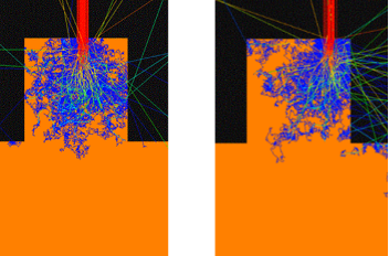
Fig. 5.6 Monte Carlo simulation result for secondary electron generation. Incoming primary electrons are indicated in red, color scale from red to orange, yellow, light blue, and dark blue indicate decreasing electron energy for both primary beam and generated electrons. Due to the short mean free path, only secondary electrons generated close to the surface will exit the sample, which results in more secondaries being emitted close to the edge (right panel).#
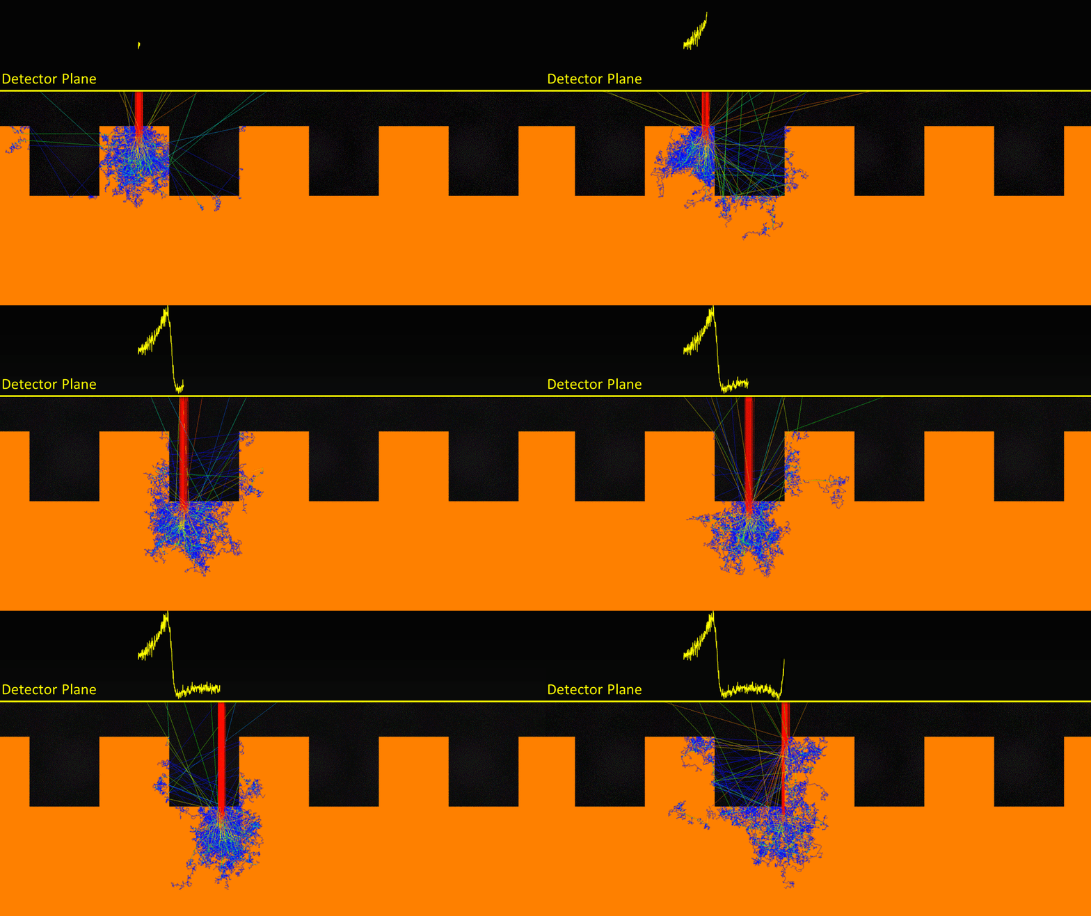
Fig. 5.7 In this simulation, all secondary electrons that hit the yellow detector plane are considered as SE signal. The graph shows how this signal develops when the electron beam is scanned over the surface. A clear change is signal is observed when the beam scans over the edge showing how SEs provide topography contrast. It can also be observed that secondary electrons may be shielded from the detector by other relief structures, e.g. for electrons generated in the well close to the edge. In practice this shielding may also depend on the position and orientation of the detector with respect to the sample giving a shadowing effect in the images. This shadowing will be more pronounced for an ETD compared to an in-lens detector and will also depend on the strength of the field attracting secondaries towards the detector.#
5.3. Backscattered electrons#
The other type of electron signal that can be detected in the SEM are back-scattered electrons. A back-scattered electron is abbreviated as BSE. The below video explains BSE detection, the contrast provided by BSEs and introduces the electron interaction volume and the generation of SE2s and SE3s.
5.4. Beam damage#
Inelastic scattering leads to the deposition of energy into the sample. After an inelastic scattering event, the incoming electron has lost part of its energy which is transferred to the sample. In the case of secondary electron creation, this energy is transferred to the secondary electron. The amount of energy lost equals the energy needed to free the electron from its orbit plus the kinetic energy of this electron after emission into the material. In the atomic model, we speak of shells as groups of orbits that are at (almost) the same energy level but in which the symmetry or orientation of the orbital motion is different. Inner shells are shells located close to the atom nucleus.
Inner-shell ionization, the emission of a secondary electron from an orbit in an inner shell, has a relatively large cross section compared to other inelastic scattering events (only interaction with plasmons and elastic scattering have a larger contribution to the total scattering cross section). The inner shell electron is ejected into the material to a so-called continuum level in which the electron is not bound to an atom anymore but can freely travel through the material. If the inner shell ionization occurs at a distance from the surface approximately equal to or smaller than the mean free path for the ejected electron, the electron may exit the material as a detectable secondary electron. Otherwise, the electron will interact again inside the material. Interactions of low energy electrons inside the sample may lead to sample damage via for instance the breaking of chemical bonds. Also other inelastic scattering processes may directly or indirectly contribute to beam damage, the damage done to the sample as a result of irradiation with the electron beam. Chemical reactions of low energy electrons are the main contributor to sample damage. Other factors that may contribute are (local) heating, (local) electric fields due to charging or separation of charges in the material, and, at high (\(>100 keV\)) incoming electron energy, direct displacement of an atom, so-called knock-on damage. In organic materials, chemical bond breakage can lead to the release of small hydrocarbon fragments and conjugation of carbon-carbon bonds. Beam damage may thus lead to chemical and structural changes evidenced for instance in atomic and molecular rearrangements, sample shrinkage, and mass loss.
5.5. X-ray and photon emission#
Inner-shell ionization leaves an unoccupied electron level relatively close to the atom nucleus. Such a vacancy will be rapidly filled by an electron from a higher shell, bringing the electron to a more stable (but still ionized) state. The energy lost by the electron decaying from the higher shell to the inner shell vacancy is released in the form of an X-ray photon. This X-ray photon thus has an energy exactly equal to the energy difference between the two shells. As energy levels are unique for each atomic element, the X-ray energy bears a unique signature of the atom that was ionized. Thus, the overall energy spectrum of X-rays emitted from the sample provides information about the elemental composition of the sample. The collection of the emitted X-ray spectrum is called Energy Dispersive X-ray Spectroscopy (abbreviated as EDX, or sometimes EDS, EDXS or XEDS).
A single atom can emit X-rays with different energies depending on the shell in which the vacancy was created and the shell from which this vacancy is filled. The shell closest to the nucleus is referred to as the K-shell (this contains the two electrons in the 1s orbital), the next is the L-shell (2s and 2p orbitals), and then the M- (3s, 3p, and 3d orbitals) and N-shells (4s, 4p, 4d, and 4f orbitals). K-shell ionization may thus lead to the decay of an electron from for instance L- or M-shell, giving rise to separate peaks in the EDX spectrum. These peaks are denoted as the K-lines (in this case Kα resp. Kß). Equivalently, an L-shell ionization can be followed by decay from M- or N-shells reflected in L-lines in the EDX spectrum. A specific atom thus gives rise to an X-ray spectrum with a characteristic distribution of peaks from which the atom(s) can be recognized. Electron irradiation of a material composed of different atomic elements then gives rise to an EDX spectrum that shows the different lines for the various elements (see Fig. 5.8).
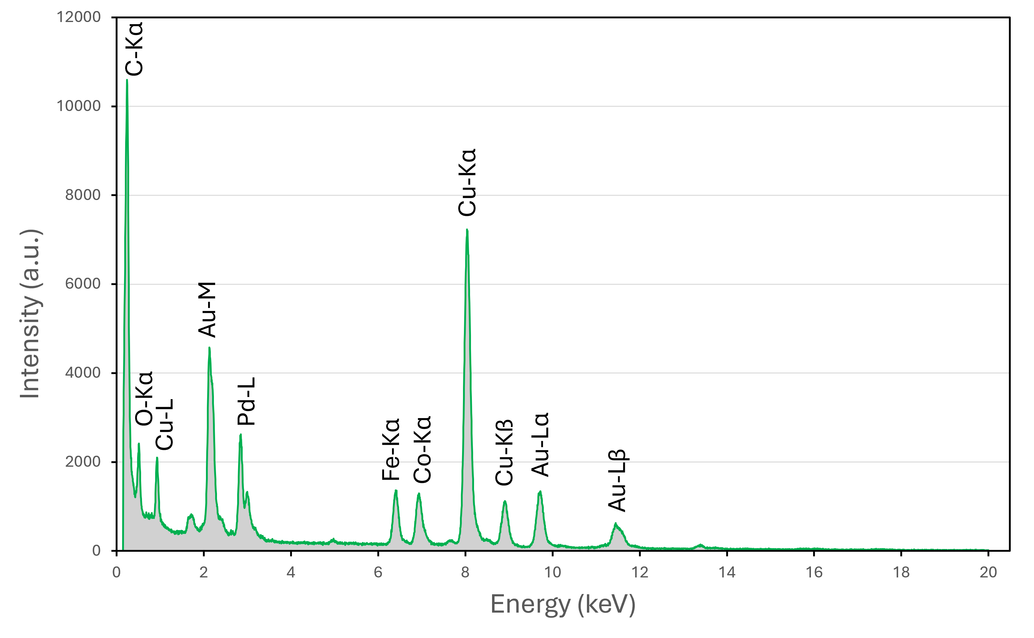
Fig. 5.8 Example EDX spectrum recorded in a TEM on a standard grating replica grid. Spectrum recorded at 80 keV electron beam energy and 0-20 keV X-ray spectral range with 5 eV energy bins. Indicated is the spectrum as recorded, without background and absorption corrections.#
The energy of emitted X-rays is in the order of keVs. The spectral (or energy) range for EDX in the SEM can thus be limited by the primary beam energy. Selecting a relatively high primary beam energy is beneficial for the EDX analysis as it allows more K- and L-lines to be recorded per atomic element in the sample and thus may allow more reliable identification of the atomic composition compared to lower beam energies. An EDX experiment leads to a hyperspectral (or multi-dimensional) data set: for each pixel a full X-ray energy spectrum is recorded. Besides showing a full spectrum recorded at a specific position (as in Fig. 5.8), one can thus also, a priori or a posteriori, decide to only record or display the value recorded in a specific energy window. Alternatively, after (automatic) identification of the elemental composition on a pixel-by-pixel basis, one can plot abundance maps for the different atomic elements present in the sample (see Fig. 5.9).
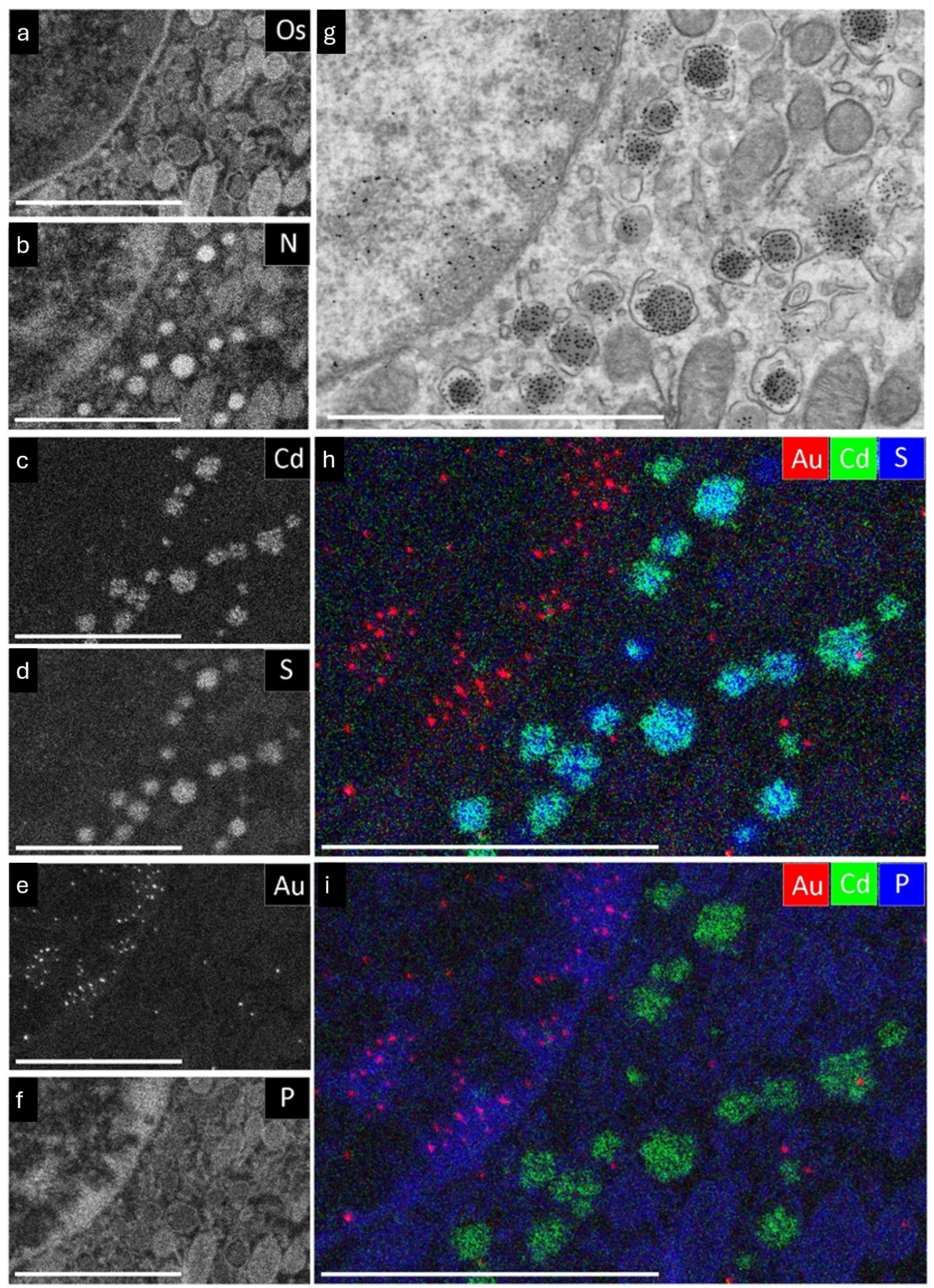
Fig. 5.9 Example of elemental mapping with EDX on rat pancreas tissue with Au nanoparticle and CdSe quantum dot immunolabelling. (a-f) Abundance maps for the different elements indicated as recorded with EDX. (g) SEM back-scattered electron signal recorded simultaneously with the EDX signals. (h-i) False color composite images obtained by adding selected elemental abundance maps. Scalebars 2 μm. Figure adapted from Scotuzzi et al, Scientific Reports 7:45970 (2017), DOI: 10.1038/srep45970, licensed under CC BY 4.0.#
A special type of X-ray emission that is not due to atom-specific interactions is Brehmsstrahlung. Brehmsstrahlung (German for ‘braking radiation’) originates from the deceleration of primary electrons upon interaction with the sample. Upon interaction with an atomic nucleus, the primary electron besides being deflected may loose some energy in the process. This energy is lost by emission of an X-ray photon. The energy range can thus span the entire X-ray window from about 0eV up to the primary beam energy. Brehmsstrahlung thus gives a near continuous background in the EDX spectrum.
Auger electrons
An alternative process to the release of an X-ray photon upon the decay of an electron to an inner-shell vacancy is the emission of another electron. In this case, the higher shell electron transfers its energy to another high-shell or valence band electron, which can then escape with a few keV energy. This process is called Auger recombination and electrons emitted in this way are referred to as Auger electrons. Like X-ray photons, the energy spectrum of Auger electrons bears information on the atomic transitions and thus the elemental composition of the sample. Due to their higher energy, Auger electrons can escape the sample from larger depth than the low-energy secondary electrons.
The filling of an inner-shell vacancy either via X-ray emission or Auger recombination (see box), still leaves the atom ionized, now with a higher-shell vacancy also called a hole. This still leaves the atom ionized but in a more stable state compared to the inner-shell ionized atom. The hole can be neutralized via decay of an electron from the conduction band or electrons travelling in continuum bands in the sample (including secondary electrons). This electron-hole recombination can give rise to the emission of a photon in the (near-)visible wavelength range. The (near-)visible range light emitted as a result of electron beam irradiation is called cathodoluminescence. Direct (intramolecular) excitation of electrons in the sample from a low energy to a higher energy state and subsequent decay, e.g. a fluorescence transition, can contribute to cathodoluminescence. Thus, if fluorescent or otherwise luminescent materials are present in the sample, their spectra may appear in the cathodoluminescence spectra. However, the cross sections for such excitations are typically very low, even compared to cross sections for processes leading to damage. Thus, for low concentrations of luminescent or fluorescent materials, damage may already occur before a detectable amount of photons have been emitted.
Interaction volume and escape depths
The interaction volume is the entire volume in the sample in which electron scattering interactions may take place upon electron irradiation. Depending on the energy of electrons still present at a specific depth in the sample, all or a subset of the discussed scattering processes may take place. Products released by these scattering processes (back-scattered electrons, secondary electrons, Auger electrons, X-ray and cathodoluminescence) may be used as signal. However, whether these can leave the sample may depend on the depth at which they are generated and their own specific interaction cross sections. For secondary electrons, we have already seen that their mean free path is relatively low and that the can only escape from regions near the sample surface. Thus, we can think of the interaction volume as composed of different layers or depths from which respective signals can be detected. However, especially in the case of secondary electrons, it should be realized that these will be generated and may thus cause damage throughout a much larger part of the interaction volume.
Characteristic X-rays can originate from deep in the sample as their interaction cross sections are incredibly small. Their sample depth is thus mostly limited by the energy that the travelling electrons still need to have in order to be able to still generate few keV X-rays. Also back-scattered electrons can originate from deep in the sample with their escape depth mostly limited by the energy of the back-scattered electron to be sufficient for the electron to travel back to the surface. Brehmsstrahlung can come from even deeper in the sample as the primary or elastically scattered electrons that do not have sufficient energy to still escape can still generate Brehmsstrahlung that may exit the sample. Cathodoluminescence can be generated with relatively low energy electron interactions and the generated photons can escape from deep in the sample. Cathodoluminescence thus has the largest escape volume.
5.6. Immersion modes & In-column detectors#
If the sample is immersed in a magnetic of electrostatic lens field, imaging is done in immersion mode. In TEM, this means the sample is inserted in between the magnetic poles of the objective lens. In SEM, magnetic immersion means the magnetic field of the objective lens extends below the objective lens pole piece into the vacuum chamber. Electrostatic immersion means the sample stage is at a different potential compared to the objective lens giving rise to an electrostatic field between sample and objective lens. The below video explains immersion mode imaging in more detail and discusses the related concept of in-column detection.
5.7. Charging#
During electron microscopy, the electron beam injects electrons in the sample. As a result of the interactions of the primary electrons, secondary and back-scattered electrons may escape from the sample. For thin samples, electrons may also leave the sample at the bottom surface. If there is an imbalance between total number of electrons injected into the sample and the total number of electrons leaving the sample, the sample may gradually charge up during irradiation. This (im)balance can be expressed in term of primary beam current and the secondary and back-scatter electrons yields of the sample. The video explains charging in more detail including its dependence on primary electron beam energy.
In case of transmission imaging, the analysis as done in the video should also include the transmission yield, the forward scattering yield and the secondary electron yield for the bottom surface. To avoid artefacts due to sample charging, the sample should be properly grounded. In case of weakly conducting or insulating samples, a thin conductive coating (e.g. a sputter-coated gold film) may prevent the occurrence of artefacts. In this case, the coating will screen the electron beam from any electric field generated by charges in the sample. However, the coating itself may impact the visibility of high-resolution features in the sample. Alternatively, careful consideration of the imaging conditions (beam energy, current, dwell time, line or frame integration) may prevent the occurrence of artefacts. Further, the energy dependence of the electron yields and the sign and magnitude of charging also impacts the contrast observed in the images, particularly in the case of secondary electron imaging. Figure Fig. 5.10 and Figure Fig. 5.11 show examples hereof. In general, one should always be aware of potential charging artefacts when imaging insulating biological materials, which can be checked by changing beam current, dwell time, scan direction, use of line or image averaging or changing the landing energy.
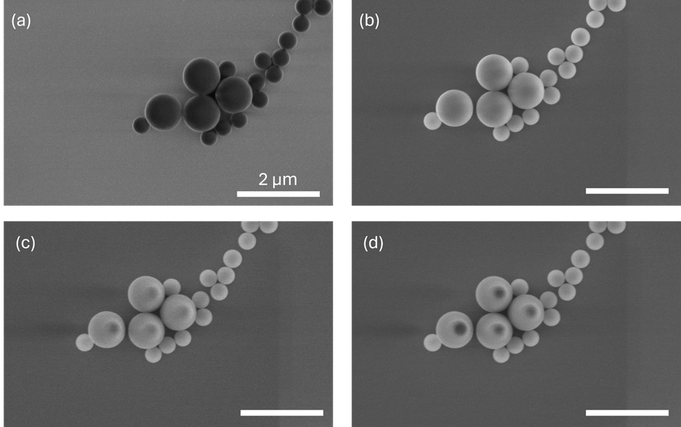
Fig. 5.10 Contrast variations and charging artefacts in SEM with secondary electron detection. Spherical SiO2 particles on a conductive, grounded indium-tinoxide (ITO) coated substrate. (a) Image recorded at 1kV beam energy, 0.1nA beam current and 200ns dwell time with 8 times image averaging. Particles appear dark with a bright outer edge due to positive charging. Note the appearance of streaking artefacts on the substrate and the apparent neck formation between the particles. (b) At 5kV beam energy (0.1nA, 200 ns, 8 times image averaging) negative charging leads to contrast inversion, artefacts are in the darker appearance of the particle core, which can be seen displaced from the center in the case of three touching spheres and the onset of streaking artefacts. (c) Image recorded with same settings as in (b) but with 1.6 µs dwell time and no image averaging. Thus the same total number of electrons as in (b) but the image averaging process with reduced dwell time allows from charge to (partially) dissipate between scans. (d) Same settings as in (c) but with 3.2 µs dwell time. Charging artefacts aggravate. Note also the asymmetric appearance of charging artefacts in the scan direction (from top left to bottom right). Images recorded with a through-lens detector, use of an in-chamber Everhardt-thornley detector may lead to even more asymmetry in the observation of charging artefacts.#
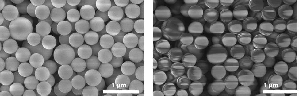
Fig. 5.11 Complex charging artefacts secondary electron images of a sample of spherical SiO2 particles on conductive, grounded ITO-coated substrate. Left: Recorded at 5 kV, 0.1 nA, 200 ns with 8 times image averaging. Right: Same energy and current but 10 µs dwell time in a single scan.#
5.8. Biological samples for EM#
Transmission imaging can only be done for sufficiently thin samples. ‘Sufficiently thin’ here not only means thin enough to allow electrons to be transmitted, but also with respect to the mean free path of unwanted (inelastic) interactions that may, e.g., lead to damage or loss of coherence. This means biological samples need to be thinned down or sectioned prior to observation with (S)TEM. We will deal with sectioning and all other steps necessary to prepare biological samples for electron microscopy in the next chapter. An advantage of sectioning is that it provides access to the cell or sample interior, and, by collecting serially cut sections, can allow for volume reconstruction. Thus, thin sections (typically 50-200 nm) are also inspected in SEM. In the case one is not interested in detecting transmitted electrons, these thin sections can be mounted on a conductive solid substrate, which, when properly grounded, can provide sufficient conductivity to avoid charging.
An advantage of SEM and detection of back-scattered or secondary electrons is that imaging is not limited to thin sections. Whole cells, thicker tissues, or even small organisms can be mounted in the vacuum chamber of the SEM. In the case of relatively thin samples like cells, mounting on a conductive substrate may again be sufficient to avoid charging especially when imaging the thinner parts of the cell like lamellipodia. For larger specimen like the beetles and bugs one often encounters as exemplary SEM images, the sample needs to be provided with a conductive coating such as sputtered gold and mounted on a grounded substrate.